|
Japanese
English |
|
Due to Professor Kawarada's retirement, this laboratory will close at the
end of March 2025,
but this website will remain available for the time being.

========================================================
You can see citations of Kawarada Lab's publications.
【Waseda pure elsevier】
【google scholar】
========================================================
Prof. Kawarada’s final lecture was held on March 8, 2025.
“Progress in Diamond Semiconductor Devices”
Email address after April 2025: 
Carbon nanoelectronics
Due to its extreme properties, diamond and carbon nanotube are expected to be applied in the ultimate semiconductor devices in high power, high temperature, high frequency operation and highly integration. In diamond, we focused on 2 dimensional hole gas (2DHG) layer appearing on a hydrogen terminated diamond surface and developed surface channel field effect transistors (FETs). This type of FET is applicable in high power and high-frequency devices, in-plane- gate FETs for single hole transistor, and biosensors in electrolyte solution. We are also investigating carbon nanotube for the multi layer interconnection for the next generation ULSI and ultimate electrode for SiC power transistors.
Research Subjects
In research, we worked on nanoelectronics from RF & power devices, superconductor devices, biosensors, bioelectronics and ULSI fabrication process based on nanocarbon electronics. The work covers the following area:
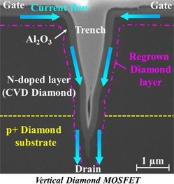
— Power and high temperature operation of diamond MOSFET using 2DHG. Blocking voltage>1500V. Constant operation at 400℃. IEEE IEDM 2014.11.02 (2014), Appl. Phys. Lett. 105 013516 (2014).
— Microwave devices and their characteristics using diamond MOSFET. fT 45 GHz, fmax 100GHz are obtained with a power handling capability exceeding those of Si or GaAs transistors. JJAP 51, 090111 (2012)
— Biosensor & bioelectronics using surface modification. Diamond solution gate FETs for Biosensing DNA detection to detect single base mismatch. Biosensor & Bioelectronics 33, 152 (2012), 40, 277 (2013)
— Carbon nanotubes grown at low temperature compatible with Si ULSI fabrication. With densely packed & vertically oriented single or double wall carbon nanotube for interconnection and super capacitor. Carbon 57, 79 (2013), 57, 401 (2013). Appl. Phys. Lett. 106 213503 (2015), 106 123501 (2015)
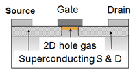
— Diamond superconductivity using highly B-doped (1021cm–3) diamond. Tc~10K enables cryoelectronics application. Phys. Rev. B 85,184516 (2012), Appl. Phys. Lett. 106 052601 (2015)
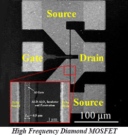
1. High power, high temperature & high frequency Diamond MOSFET

Appl. Phys. Lett., 81, 2854 (2002) |
|
- Break down > 2000V
- T : 400℃
- fT : 45GHz
- fmax 100GHz
- IDSmax : 1.2A/mm
- IEEE Elect. Dev. Lett, 22, 390(2001), 23, 121(2002), 25, 480(2004)
- Appl. Phys. Lett. 88, 112117 (2006)
- IEEE IEDM p.873 (2007)
- APEX 3, 044001 (2010)
- JJAP 51, 090111 (2012)
- IEEE IEDM p.279 (2014) Appl. Phys. Lett.109. (2016)
|
2. Superconductivity and transistor application
 |
|
- Highly B-doped >1021cm-3
- Diamond Tc ~10K
- Cryoelectronics
- Y.Takano, H.Kawarada, et al. Appl. Phys. Lett. 85, 2851 (2004)
- T.Yokoya, H.Kawarada, et al. Nature, 438, 647-650 (2005)
- Phys. Rev. B. 82, 085318 (2010)
- Phys. Rev. B. 85, 184516 (2012)
|
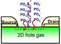
3. Biosensor & bioelectronics
 |
|
- Surface chemical modification
- Diamond solution gate FETs for Biosensing DNA & protein detection
- Phys.Rev.E. 74, 041919 (2006)
- Appl. Phys. Lett. 90, 063901 (2007)
- J. Am.Chem Soc. 130,13251 (2008)
- IEEE IEDM (2008)
- Biosenser & Bioele, 26, 1599 (2010), 33,152 (2012), 37 (2012)
|
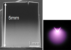
Carbon nanotubes
 |
|
- Densely packed & vertically oriented single or double wall carbon nanotube for interconnection and super capacitor
- State of art plasma
deposition
- Carbon, 44, 2009 (2006)
- J. Phys. Chem. B, 111, 1907 (2007)
- Nano Letters 8 886 (2008)
- carbon 45,825 (2010)
- Appl. Phys. Lett. 106.123501 (2015)
- Appl. Phys. Lett. 106.213503 (2015)
|
|
|